ASUS P5N- E SLI REVIEW BENCHMARK AND OVERCLOCKING CHIPSET NFORCE 650I SLI
![]()
|
|
 |
|||||||||||||||||||||||||||||||||||||||||||||||||||||||||||||||||||||||||||||||||||||||||||||||||||||||||||||||||||||||||||||||||||||||||||||||||||||
| Posted:2007-03-07 By chipset review Number of View:56506 |
||||||||||||||||||||||||||||||||||||||||||||||||||||||||||||||||||||||||||||||||||||||||||||||||||||||||||||||||||||||||||||||||||||||||||||||||||||||
By :chipset review Posted:2007-03-07
The released by NVIDIA company chipset for processors family intel core 2 caused ambiguous emotions. Certainly, from the side formal characteristics it not equal to NVIDIA nForce 680i SLI . On its possibilities this chipset, actually exceeds alternative solutions from Intel and, already from AMD. . Both the products (680i-650i), built in reference design and ASUS striker extreme, have a set of small problems. But in this case the price of motherboards, based on high end collection from NVIDIA is about 100$ higher. Company NVIDIA begin the delivery to motherboard producers , the new chipset nForce 650i SLI, This version is not so attractive as NVIDIA nForce 680i SLI. . Thus, taking in account NVIDIA nForce 680i SLI specification , from the new chipset it is possible to expect the excellent combination of consumer characteristics and price. Specifically, therefore our laboratory decided to pay attention to one of the first appeared on the market motherboards in the base of NVIDIA nForce 650i SLI, ASUS P5N- E SLI. However, before passing to the examination that of this large hopes solution, it is necessary to say pair of words about chipset NVIDIA nForce 650i SLI, As u already know such chipset it not positioned as high end solution, but in the average price range, it has a certain reduction in its possibilities. 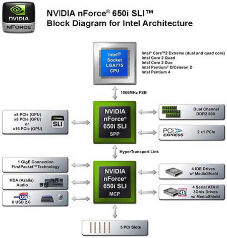 As u see, the main difference NVIDIA between nForce 650i SLI from 680i SLI is in the decrease in the quantity of lines PCI express, which is reflected in the diagram for the realization of SLI technology . While nForce 680i SLI had at its disposal the whole 46 lines PCI express, in nForce 650i SLI there are only 18. As a result, while elder model chipset proposes SLI technology according to : PCI express x16 + PCI express x16, allowing moreover and additional PCI express x8 for installation of physical accelerator, in nForce 650i SLI technology SLI uses a simpler diagram PCI express x8 + PCI express x8. nForce 680i SLI and nForce 650i SLI are built on the base of the same north bridge c55 SPP, their south bridges are different . The functions of this microcircuit in nForce 650i SLI are strongly reduced, and not only by the deprivation of support to more lines PCI express. Thus, NVIDIA nForce 650i SLI has only one gigabit net controller instead of two in elder model , four Serial ATA-300 by ports instead of six and eight ports USB 2.0 instead of ten. Then nForce 650i SLI proposes two channels parallel ATA-133, witch for contemporary chipsets is rarity. The south bridge in nForce 650i SLI use the microcircuit nForce 430 MCP, witch is well familiar to us on the integrated chipset nForce 6150. It is necessary to add that the part of possibilities in nForce 650i SLI is opened at BIOS level . The same northern bridge in nForce 650i SLI, don\'t has official support to the technology NVIDIA linkboost and support to high-speed memory with EPP.
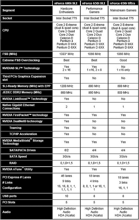 Actually, if the absence SLI support according to : PCI express x16 + PCI express x16 is not for you fundamental , then, judging by characteristics, the chipset NVIDIA nForce 650i SLI can become the completely valuable system. And it can be considered as real competitor for Intel p965. Specification and delivery setThe first motherboard, based on NVIDIA nForce 650i SLI is ASUS P5N- E SLI. 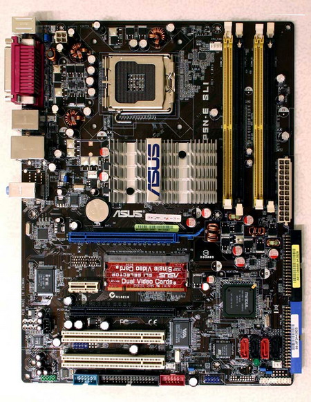
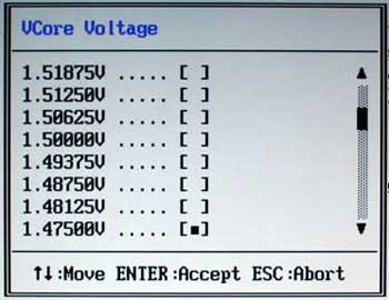
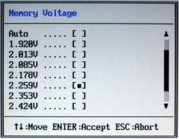
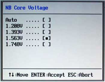
From the basic formal specification it is not inferior to motherboards built in iP965. In this case it is necessary to understand, that ASUS P5N- E SLI relates to the category of inexpensive motherboard. . Thus, this motherboard cost today $120-140. The Motherboard ASUS P5N- E SLI is proposed in the standard size box without beautiful pictures. 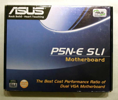 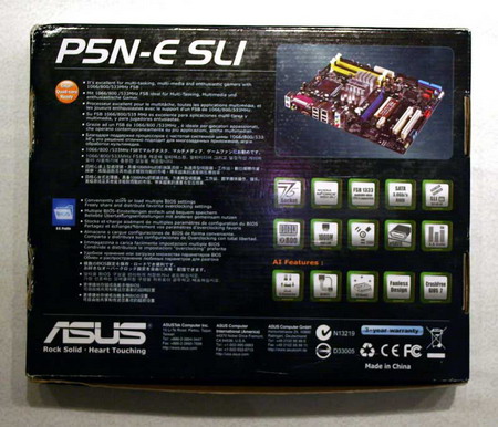 Inside the box we find the motherboard :-), management CD and drivers, cable for connection of disk drive and Parallel ATA devices, two Serial ATA cable and the corresponding power adapter . 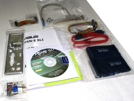 All necessary part are present in the box as standard for this price range. More detail about ASUS P5N- E SLI possibilitiesThis motherboard support all LGA775 processors, including dual core and four core processor CPU family core 2. More there are no official data about the support of future processors with system bus frequency 1333 MHz, but there are no doubt that such support will be added in next bios update. This can be concluded from the overclocking capability from one side, and by the use of north bridge c55 SPP (which in the composition of chipset NVIDIA nForce 680i SLI officially support future system bus) . 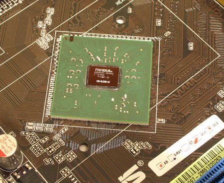 He other words, there are no reasons, which can cause problems in the operation of ASUS P5N- E SLI with future processors. As far as work with memory is concerned, here ASUS P5N- E SLI differs a little from the same ASUS striker extreme i680. Due to the properties of north bridge c55 SPP , the frequency DDR2 SDRAM can be set as dividers relative to FSB frequency (This collection of dividers is not too rich and includes FSB:DRAM 1:2, 5:8, 3:4 and 1:1). It is necessary to note that despite to the promised by NVIDIA limitation in the part of support to technology EPP by chipset nForce 650i SLI, ASUS P5N- E SLI support it without problems. Separate attention should be given to existing on motherboard two slots PCI express x16. These slots are necessary exclusively for using a pair of video card , working in regime SLI. With the start of this regime both slots will be switched to PCI express x8. But if in the system is installed only one video card, then the first slot functions as valuable PCI express x16, and the second is disconnected. 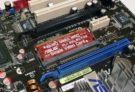 Because of the south bridge nForce 430 motherboards ASUS P5N- E SLI have eight ports USB 2.0, four ports SATA-300 with support to capacity 3 Gbit in second, NCQ and RAID, two channels PATA-133 and gigabit net port. 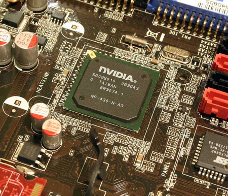 These possibilities are supplemented with the aid of VIA VT6308P controller , which ensures the work of two IEEE1394 ports, and the chip jMicron JMB360, which adds a number of properties to the motherboard : the support of additional port eSATA (SATA on-the-Go, as it is called BY ASUS). The six-channel integrated sound on ASUS P5N- E SLI is realized through codec the high resolution realtek ALC833. Although this codec possesses the support of 8 channels, on the motherboard are brought out only six of them. Furthermore, it should be noted that this codec relates is inexpensive and do not possesses high quality of support EAX 2.0 for example. Design and impressionAssembly of ASUS P5N- E SLI and its declared possibilities did not produce special impression . All is completely typical for motherboard average price range. But as far as design is concerned, here the product in question revealed completely remarkable and sufficiently uncommon special features. Thus, the first is the large aluminum radiator, installed on the north bridge chipset. 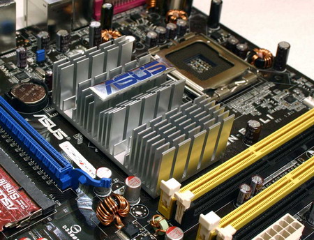 The tendency of developers to reduce the final cost of motherboard gave did not give ASUS P5N- E SLI chance to get more effective cooling construction.. As u already know the chip c55 SPP strongly heat during load. Th aluminum radiator installed on this motherboard could not keep with such temperatures. So that we would recommend in first place to replace this cheap radiator by something more effective, especially, if you plan to overclock, or if your system does not provide good air circulation in the region of north bridge. On the south bridge of this motherboard there are no cooler installed. Doubtful savings on radiators touched not only chipset microcircuits . There is no effective cooling and the power converter of processor, which on ASUS P5N- E SLI was made according to classical three-channel diagram. In this case this diagram contains neither digital feedback nor SMT capacitors, which is completely regular , taking in account the low cost of this motherboard. In the voltage converter are used the usual chemical capacitors from the production Of united chemi-Con.... 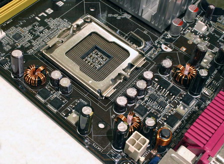 The elements of power converter for processor, including capacitors, are located on the printed-circuit board but not in the most successful war : they are placed directly around the processor . As result, they are capable of depriving installation on ASUS P5N- E SLI of cooling systems with massive base. Another problem that can rise with the connection to the motherboard of the additional 12- voltage power cable . This motherboard is equipped with 4- with contact pin, contemporary has eighth contact plug . 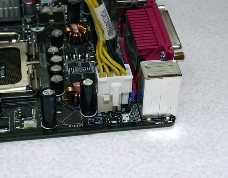 It is necessary to say that the design of ASUS P5N- E SLI have some other deficiencies, many of which can be seen on the following picture . 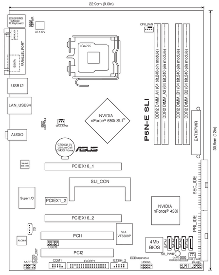 All problems with the unsuccessful selection of place for distribution of various port on the motherboard can be explained by the reduced (for savings purpose ) area PCB, and this give ASUS engineers a certain justification. so we add that P5N- E SLI offer only three fan connection . For motherboard of this level, ( which has many heating elements ), this is insufficient. On The rear panel we find the PS/2 ports for mouse and keyboard connection , four ports USB, port IEEE1394, net joint RJ45 with the diagnostic light-emitting diodes, port eSATA, three analog audio- port, coaxial SPDIF and parallel port.  BIOSThe overclocking possibilities of motherboard mainly are determined by its BIOS. Taking in account that at the base of ASUS P5N- E SLI lies the same north bridge, which serves as base for ASUS striker extreme, we expected that BIOS Setup of this motherboard will propose similar possibilities for processors and memory overclock . However, it was not there. ASUS engineers substantially limited the number of BIOS Setup setting in their inexpensive motherboard, built on chipset NVIDIA nForce 650i SLI. Remains only to hope that the overclocking potential of motherboard will not be affected by large value. All BIOS setup possibilities , are setting and configuration of memory and processor ( their overclock ),those setting are located in menu advanced. Major portion of overclockers parameters are in the division jumperFree configuration. 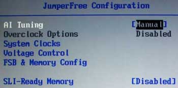 Here it is possible to turn off technologies EPP, and also to get in setup page with the functions for control of voltage and frequencies.  The subsection system clocks contains only option for the task of frequency system bus PCI express, which varies in the limits from 100 to 131 MHz with 1 MHz. step. 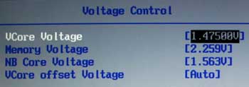 In the subsection voltage control we have access to control three values:
In the subsection FSB & memory config we have access to the frequency of system bus FSB and memory system bus . 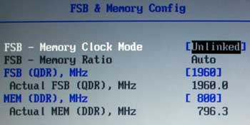 FSB can be set in the frequency limits from 133 to 750 MHz. The frequency of memory is advanced with FSB, using dividers FSB:DRAM equal 1:2, 5:8, 3:4 and 1:1. NVIDIA nForce 650i SLI does not have a completely asynchronous generator for memory system bus . After the installation of the desired value in BIOS Setup the motherboard chose the most suitable divider and will indicate the actual memory frequency . In the majority of the cases this frequency differ from the desired one by not more than 10-20 MHz in the smaller side. However, the range of memory frequencies , which is allowed by ASUS P5N- E SLI in asynchronous regime varies from 400 to 2600 MHz. 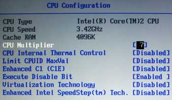 The division CPU configuration opens access to the manipulation with the multiplication factor of processor and to control different processor technologies. All memory settings are found in the subsection memory timings settings in the chipset division . 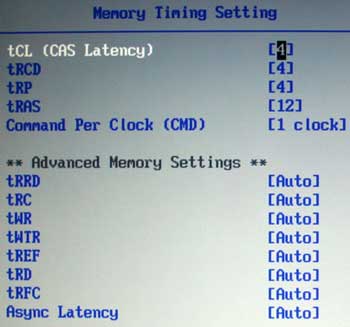 As u see, This last section opens access to all basic latency of memory subsystem , it also allow to control the parameter command rate. It is necessary to note that practically all enumerated voltage, and also processor and memory setting , can be set in value auto, that somewhat simplifies BIOS Setup. Besides the possibilities, aimed directly at overclocking, BIOS Setup in ASUS P5N- E SLI has a pair of other curious possibilities. First, allow to preserve setting profiles in the energy-independent memory and even in files. Second, is the build in utility EZ flash 2, as basic function of which comes out the update of bios, without leaving the BIOS. This utility is capable of new bios file from floppy, CD and hard disks, marked under FAT, and also from USB flash disks. The hardware monitoring, realized on ASUS P5N- E SLI, allow to track the fans rotation speed and processor , motherboard temperature 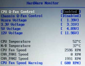 IN This BIOS we found also the traditional technology Q -Fan, which allow to control the fan speeds depending an system temperatures . OverclockingFrom this BIOS setup description it is clear that ASUS P5N- E SLI don\'t present a rich tuning as many other motherboards. At the same time all basic parameters are present and can be edited , and this give us hope for its applicability as overclocker platform. For our overclocking experiments we used a system, based on ASUS P5N- E SLI with processor intel core 2 Extreme x6800 . In addition to this, in the test platform we used 2 Gb DDR2 corsair TWIN2X2048-8500C5D, video card powerColor x1900 XTX 512MB and hard disk western digital raptor WD1500AHFD. during the tests DDR2 SDRAM always operated at frequency, equal or only less than 800 MHz with latency 4- 4- 4- 12-1T. For cooling the processor we used the cooler zalman CNPS9500 LED, and, furthermore, we installed on the radiator of north bridge additional 60 mm fan. The operational stability of the system indicated with overclock was checked with the aid of the well recommended utility ORTHOS, based on prime95 code . The maximum system bus (FSB) frequency , with which the motherboard preserves capability for stable functioning, was found rapidly. Just as with tests ASUS striker extreme, it was 490 MHz. 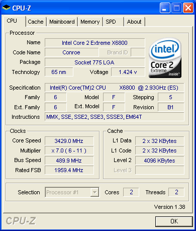 For reaching this result for us it was necessary to only increase voltage on the north bridge to 1.563 v and on processor to 1.475 v. all is so simple. ASUS already for long time released motherboard, on which all overclocking function work immediately. First, we should note that such high result with frequency FSB was succeeded only because of the additional fan, which we installed in the radiator of north bridge. With the removal of this fan the motherboard just refuse to POST even with reduction in the frequency FSB to 450 MHz. In the second place, as showed tests, such high frequencies FSB on ASUS P5N- E SLI as on ASUS striker extreme, has a little sense . The switching FSB strap somewhere in the region 400-450 MHz with the passage to this boundary catastrophically falls in performance of memory subsystem , which then, is not compensated even by considerable increase in the processor clock frequency . And third, with the tests of ASUS P5N- E SLI we encountered one problem, called FSB overclocker . Th motherboard examined by us demonstrated its complete unfitness for work with the installation of FSB frequencies in the range from 400 to 450 MHz. To this it is necessary to add that P5N- E SLI do not set the seen in bios voltage . In particular, real voltage on processor proves to be that below the set in BIOS Setup approximately on 0.05 v. Asynchronous memory in chipset nForce 650i SLI allow also to overclock the DDR2 SDRAM, which can have frequency completely independent from the frequency FSB. We decided to check this value limit will using memory modules TWIN2X2048-8500C5D with voltage 2.4 v. here we got a certain disappointment: ASUS P5N- E SLI, as it seemed, overclock DDR2 SDRAM worse than Striker extreme. The maximum achieved by us frequency on the memory system bus was 550 MHz. 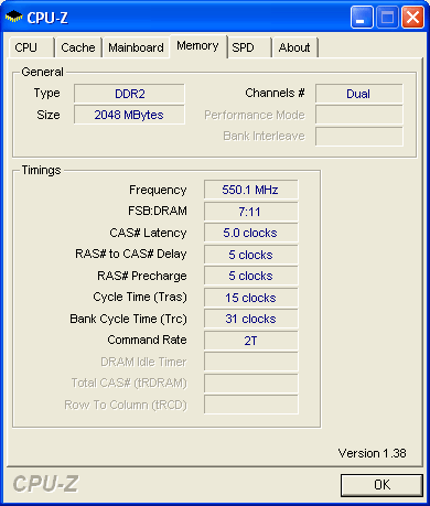 Let us recall, that on motherboard ASUS striker extreme the same modules without problems operated at frequency 587 MHz. However, there is some hope that the overclock of memory over the long term will be improved with the release of new BIOS versions . Performance TestingSince that examined by us today is motherboard ASUS P5N- E SLI based on chipset NVIDIA nForce 650i SLI, which earlier we did not test, we are interested on its performance. Therefore we decided to compare the operation speed of ASUS P5N- E SLI with the speed of other popular motherboards from chipsets AMD, Intel and NVIDIA. In the composition of test systems we used the following equipment:
We tried to place all tested system in identical conditions; therefore in all platforms memory operated at frequency 400 MHz with latency 4- 4- 4-12. . The motherboards, based on chipset intel, as is known, do not allow to change the command rate . Therefore, platforms i975X and iP965 worked with 2T Command rate.
here is the chart list :-) As show tests, the performance of ASUS P5N- E SLI is only insignificantly lower than speed of motherboard with higher class as ASUS striker extreme. In other words, this motherboard is about similar to higher class one However, we cannot forgot that the regime SLI realized on ASUS P5N- E SLI is somewhat reduced version, with the use of system bus PCI express x8. Accordingly, with the installation in the system on the base of this motherboard of pair video card, it will show perceptibly lower performance than ASUS striker extreme, which supports valuable SLI. The level of delay in this case reaches 20% in the most contemporary gaming applications. ConclusionsASUS P5N- E SLI is not deprived of deficiencies. However, this board based on NVIDIA nForce 650i SLI, can become excellent base for Core 2 systems average level. ASUS P5N- E SLI is capable of becoming alternative to the popular products, based on chipset iP965. In its price category ($120-$140) this motherboard provides good functionality, good performance and completely acceptable possibilities for processor overclock . more that, this motherboard allow to exploit video card on chips NVIDIA in regime SLI, although with a certain speed loss in comparison with the more expensive motherboard, based in nForce 680i SLI,. Pluses:
Minuses:
we would be happy to answer for your question . if you have suggestion or comment
regarding this review our support would be glad to help just join our forum and ask u will get the best answer
to discuss check our forum section :-) RATE THIS REVIEW | ||||||||||||||||||||||||||||||||||||||||||||||||||||||||||||||||||||||||||||||||||||||||||||||||||||||||||||||||||||||||||||||||||||||||||||||||||||||
![]()

ASUS P5N- E SLI review benchmark and overclocking chipset nforce 650i sli
ASUS P5N- E SLI review benchmark and overclocking chipset nforce 650i sli


7600gt review
7600gt is the middle card range.
We already benchmarked this video card and found that ...

 geforce 8800gtx and 8800gts
  Xtreview software download Section
  AMD TURION 64 X2 REVIEW
  INTEL PENTIUM D 920 , INTEL PENTIUM D 930
  6800XT REVIEW
  computer hardware REVIEW
  INTEL CONROE CORE DUO 2 REVIEW VS AMD AM2
  INTEL PENTIUM D 805 INTEL D805
  Free desktop wallpaper
  online fighting game
  Xtreview price comparison center

- The new version of GPU-Z finally kills the belief in the miracle of Vega transformation
- The motherboard manufacturer confirms the characteristics of the processors Coffee Lake
- We are looking for copper coolers on NVIDIA Volta computing accelerators
- Unofficially about Intels plans to release 300-series chipset
- The Japanese representation of AMD offered monetary compensation to the first buyers of Ryzen Threadripper
- This year will not be released more than 45 million motherboards
- TSMC denies the presentation of charges from the antimonopoly authorities
- Radeon RX Vega 64 at frequencies 1802-1000 MHz updated the record GPUPI 1B
- AMD itself would like to believe that mobile processors Ryzen have already been released
- AMD Vega 20 will find application in accelerating computations
- Pre-orders for new iPhone start next week
- Radeon RX Vega 57, 58 and 59: the wonders of transformation
- ASML starts commercial delivery of EUV-scanners
- The older Skylake processors with a free multiplier are removed from production
- Meizu will release Android-smartphone based on Helio P40
- AMD Bristol Ridge processors are also available in American retail
- The fate of Toshiba Memory can be solved to the next environment
- duo GeForce GTX 1080 Ti in GPUPI 1B at frequencies of 2480-10320 MHz
- New Kentsfield overclocking record up to 5204 MHz
- Lenovo released Android-smartphone K8


computer news computer parts review Old Forum Downloads New Forum Login Join Articles terms Hardware blog Sitemap Get Freebies

